I-V measurements
Useful for evaluating conduction, contact behavior, leakage, nonlinear response, and basic device functionality.
Metrology • Structure • Device Physics
Characterization is what turns fabrication into an experimental feedback loop. A process creates a structure; measurements tell us what was actually produced, how the material responded, and whether the device behaves as intended. This page brings together the structural, surface, thin-film, electrical, and low-temperature techniques I have used across materials research and device fabrication.
Why It Matters
Characterization is often presented as a list of instruments: SEM, AFM, XRD, profilometry, ellipsometry, electrical transport, and so on. In practice, the more important decision is choosing the measurement that can distinguish between competing explanations for a process or material behavior.
If an etch profile changes, SEM may reveal the geometry. If a film thickness drifts, ellipsometry or reflectometry may identify it. If a superconducting film has the correct crystal structure but a degraded transition temperature, electrical transport provides a different piece of the story.
The most useful understanding usually comes from combining several complementary measurements rather than relying on one technique in isolation.
Process Metrology
Waiting until the end of a long process to characterize the device can make troubleshooting unnecessarily difficult. Intermediate measurements provide checkpoints that show whether the process is still within its expected window.
Thickness, roughness, feature dimensions, etch depth, surface morphology, and profile can all be monitored before additional processing hides the information.
Electron Microscopy
SEM is one of the most useful tools in micro- and nanofabrication because it provides direct information about feature geometry at dimensions that optical microscopy cannot resolve.
Depending on the sample and imaging conditions, SEM can reveal critical dimensions, line-edge quality, residues, mask erosion, sidewall behavior, pattern collapse, surface defects, and other fabrication outcomes.
A top-down image can show whether a pattern has the intended lateral geometry, but it may not reveal what is happening through the depth of the structure.
Cross-sectional imaging can expose sidewall angle, undercut, dielectric coverage, buried voids, layer thickness, and profile evolution that may be invisible from the surface.
Surface Metrology
AFM maps surface topography by scanning a sharp probe across the sample and monitoring the interaction between the tip and the surface.
It is particularly useful when nanometer-scale roughness, morphology, step height, or local surface features matter more than lateral imaging over a large field of view.
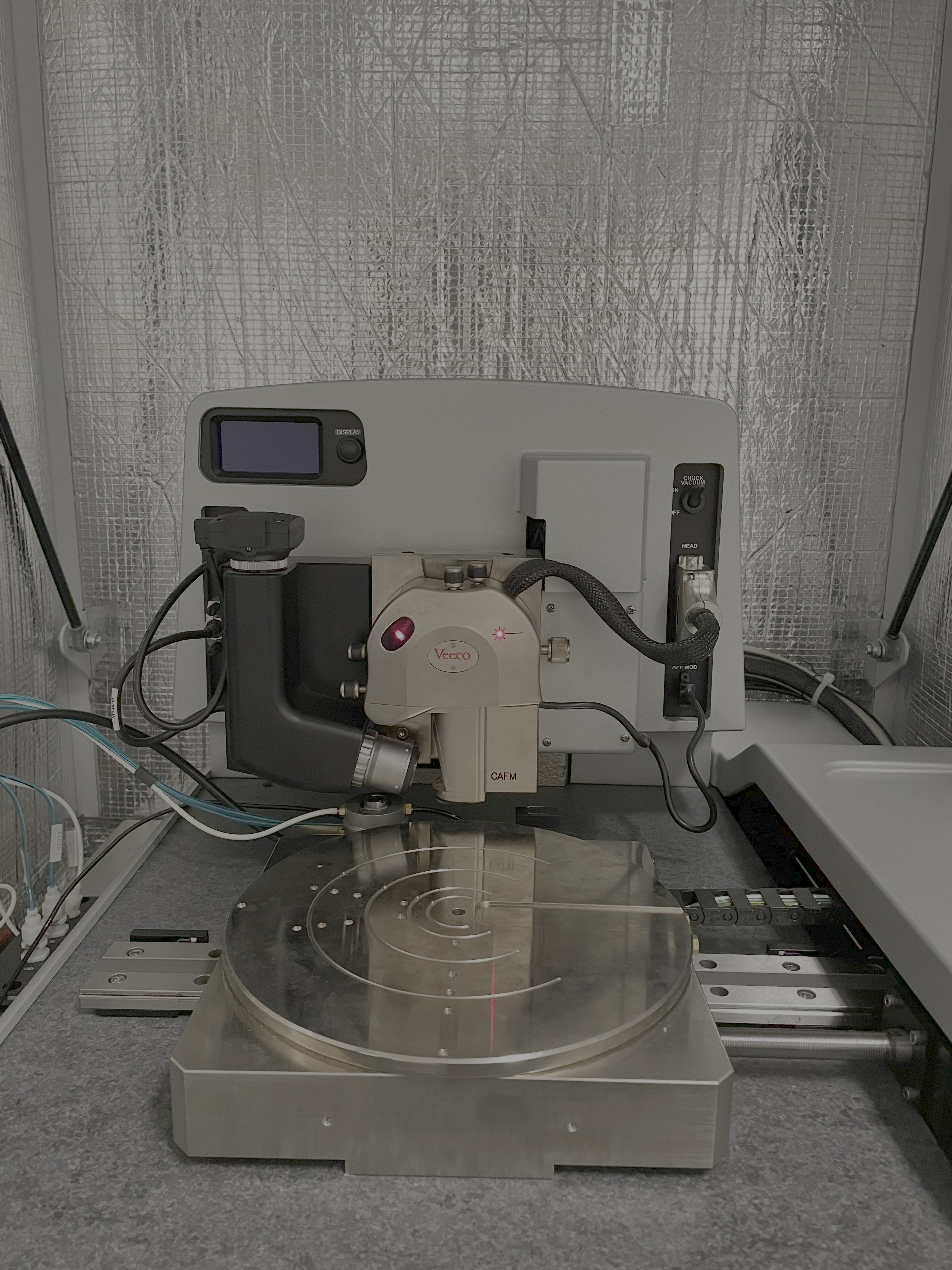
Metrics such as RMS roughness or average roughness provide useful summaries, but they do not fully describe the morphology. Two surfaces can have similar roughness values while containing very different feature sizes, spatial distributions, or isolated defects.
I therefore find it useful to examine both quantitative roughness metrics and the actual topography when interpreting AFM data.
Step Height & Topography
Profilometry provides a direct way to measure step height and surface topography over larger lateral distances than AFM.
In process development, it can be useful for measuring deposited film thickness, etched depth, resist thickness, or larger-scale surface variation.
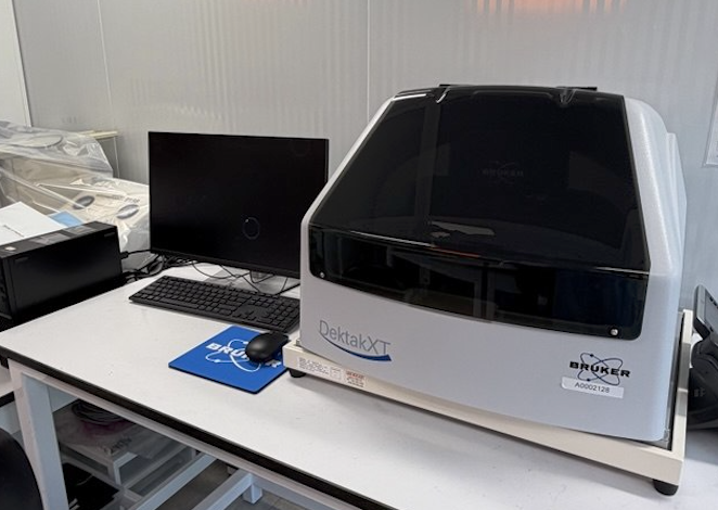
Profilometry is a good example of why the most sophisticated instrument is not always the most useful one. If the process question is simply whether an etch removed the expected depth, a well-prepared step-height measurement can provide the answer quickly and directly.
Thin-Film Metrology
Optical thin-film metrology provides a non-destructive way to extract information about film thickness and, depending on the model and material system, optical constants.
These techniques are especially useful for monitoring dielectric deposition and other thin-film processes where repeatability and thickness control matter.
Ellipsometry does not simply output a thickness independently of assumptions. The result depends on the optical model used to describe the substrate, film stack, roughness, and optical constants.
A mathematically good fit is therefore not enough by itself. The model should also make physical sense for the actual sample.
Crystal Structure
XRD was a central characterization technique during my PhD work on epitaxial superconducting oxide thin films. Diffraction provides information about crystal structure, orientation, phase purity, lattice parameters, and structural quality.
For epitaxial films, the presence and position of diffraction peaks can help determine whether the intended phase formed and whether secondary phases or structural changes appeared during growth.
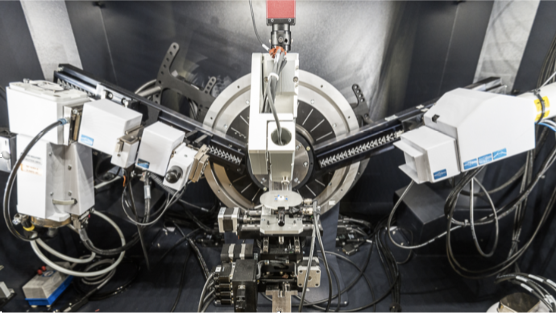
A rocking curve probes the angular distribution of crystallographic orientation around a diffraction peak. The width of the rocking curve can provide information about mosaicity and the degree of out-of-plane crystalline alignment.
As with most structural metrics, however, one number should not be interpreted in isolation. Peak shape, background, film thickness, substrate contribution, and the rest of the diffraction pattern provide important context.
Electrical Characterization
Electrical characterization translates a fabricated structure into functional information. Resistance, current-voltage behavior, Hall response, leakage, transition temperature, and field dependence can reveal whether a device or material behaves as intended.
Electrical measurements are particularly powerful because they can expose problems that are not obvious from structural inspection alone.
Useful for evaluating conduction, contact behavior, leakage, nonlinear response, and basic device functionality.
Can reveal phase transitions, superconducting behavior, metallic or insulating trends, and temperature-dependent transport mechanisms.
Provide information about carrier response to magnetic field and can be used to investigate carrier density, sign, mobility, and more complex transport behavior.
Field-dependent transport can probe superconductivity, quantum transport, scattering, and the relationship between electronic behavior and magnetic field.
Cryogenic Transport
Low-temperature transport formed a major part of my PhD research. Using cryogenic measurement systems such as a PPMS makes it possible to study electrical response across temperature and magnetic field while maintaining controlled experimental conditions.
These measurements were essential for investigating superconducting transitions, Hall response, magnetoresistance, quantum-interference effects, and other transport phenomena in electron-doped cuprate devices.
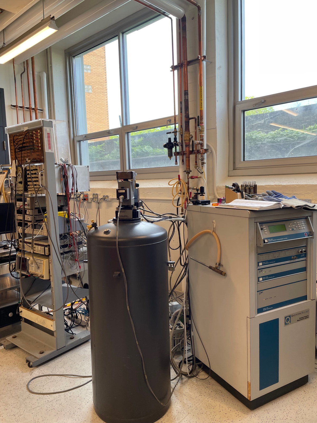
Low-temperature electrical measurements can be sensitive to contact resistance, wiring configuration, excitation current, thermal stabilization, magnetic-field history, noise, and measurement geometry.
A transport curve therefore reflects both the physics of the sample and the quality of the experimental configuration used to measure it.
Complementary Evidence
XRD, SEM, AFM, profilometry, and cross-sectional analysis reveal what material or geometry was actually produced.
Thickness, profile, roughness, uniformity, and interfaces provide feedback on whether the fabrication step remained within its intended process window.
Electrical, magnetic, optical, or low-temperature measurements reveal whether the final material or device performs as intended.
Troubleshooting
When a process fails, characterization is most useful when it helps eliminate possible causes. If thickness is correct, one hypothesis disappears. If SEM shows the lithography transferred correctly, attention can move downstream. If structural quality remains unchanged but electrical behavior degrades, the problem may lie at an interface or contact rather than in the bulk material.
This is why I prefer to choose measurements based on the failure mechanism being tested rather than collecting data simply because an instrument is available.
Practical Lessons
Intermediate process measurements can preserve information that becomes impossible to recover after additional layers are added.
Characterization is most powerful when the expected result would distinguish between specific possible failure mechanisms.
Structural, surface, thickness, and electrical measurements can reinforce or challenge one another and produce a more complete interpretation.
A precise measurement or excellent numerical fit is useful only when the interpretation is consistent with the actual material, geometry, and process history.
Continuing Notes
I plan to continue expanding this page with deeper notes on microscopy, thin-film metrology, X-ray diffraction, electrical transport, low-temperature measurements, data interpretation, and the use of characterization in process troubleshooting.