Lithography & Pattern Transfer
Electron-beam lithography, photolithography, direct-write and DUV-patterned processing, combined with dry etching, ion milling, lift-off, and feature-transfer optimization.
Explore nanofabrication →Physics • Nanofabrication • Semiconductor Devices • Quantum Technology
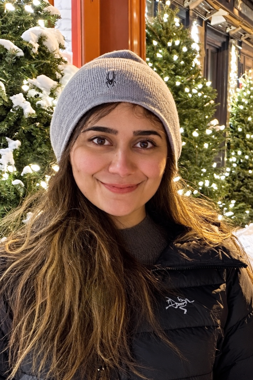
I am a physicist and nanofabrication engineer interested in how materials, fabrication processes, and device physics come together to create semiconductor and quantum technologies. This site is where I share what I have learned through research, cleanroom work, and continued exploration of nanoscale science and engineering.
Expertise
My experience spans nanoscale patterning, plasma processing, thin-film deposition, metrology, process integration, and troubleshooting across semiconductor and quantum-device fabrication.
Electron-beam lithography, photolithography, direct-write and DUV-patterned processing, combined with dry etching, ion milling, lift-off, and feature-transfer optimization.
Explore nanofabrication →ALD, PECVD, RF/DC sputtering, e-beam and thermal evaporation, pulsed laser deposition, thermal processing, and multilayer integration for functional device structures.
Explore thin films →Development and refinement of complex multi-step fabrication flows with emphasis on reproducibility, process windows, yield improvement, root-cause analysis, and corrective actions.
SEM, AFM, profilometry, ellipsometry, reflectometry, XRD, structural analysis, electrical transport, and low-temperature characterization used to validate process outcomes.
Explore characterization →Experience
In industry, I have worked across complex GaN-based microLED fabrication flows involving lithography, dry etching, dielectric passivation, metallization, thin-film deposition, thermal processing, metrology, and device integration.
My work has included process optimization, troubleshooting yield-limiting failure modes, evaluating alternative process approaches, and coordinating fabrication across multiple cleanroom facilities.
During my PhD in condensed matter physics, I developed and characterized superconducting thin films and nanoscale devices for quantum-transport experiments.
This work combined epitaxial thin-film growth, lithography, nanofabrication, structural characterization, and low-temperature electrical measurements, giving me a strong foundation at the intersection of materials science, device physics, and fabrication.
Technical Capabilities
EBL · Photolithography · Direct-write · DUV processing · Lift-off
ICP-RIE · RIE · Ion milling · Wet etching · Pattern-transfer optimization
ALD · PECVD · RF/DC sputtering · E-beam evaporation · Thermal evaporation · PLD
Process integration · RCA · Yield improvement · SEM · AFM · Profilometry · Ellipsometry · XRD
Research & Writing
My academic research focuses on unconventional superconductivity, quantum transport, electron-doped cuprates, superconducting thin films, and nanoscale devices.
PhD in Condensed Matter Physics
Explore physics & research →I write about nanofabrication, electron-beam lithography, semiconductor processing, superconductivity, and experimental physics.
Read my articles →Beyond the Lab
Science is a large part of my life, but curiosity does not stop at the laboratory. Outside of physics and nanofabrication, I enjoy painting, reading, learning languages, and exploring ideas through creative projects.
Painting gives me a different way to experiment with patterns, structure, color, and abstraction — without needing a cleanroom.
Explore my art →A collection of books, ideas, and subjects that have caught my attention beyond my scientific work.
Explore my bookshelf →Languages have long been one of my interests. I also created a YouTube channel teaching French to Persian speakers, combining language learning with my interest in teaching and communication.
Visit my YouTube channel →I am interested in advanced nanofabrication, semiconductor processing, quantum-device fabrication, and process integration.